

Support
ING918X evaluation Boards User Manual
- Categories:Getting Started
- Time of issue:2022-11-17 12:19:36
- Views:0
1、 Overview
This document introduces the hardware resources and usage of Ingchips ING91881B evaluation board, so that the R&D engineers can understand the hardware resources of ING9188 series chips and test their functions, and master the use of ING9188 series chips as soon as possible.
2、Hardware resource
The ING91881B evaluation board is shown in the figure below, mainly including temperature and humidity sensors, acceleration sensors, buttons, LEDs, buzzers and other related resources.
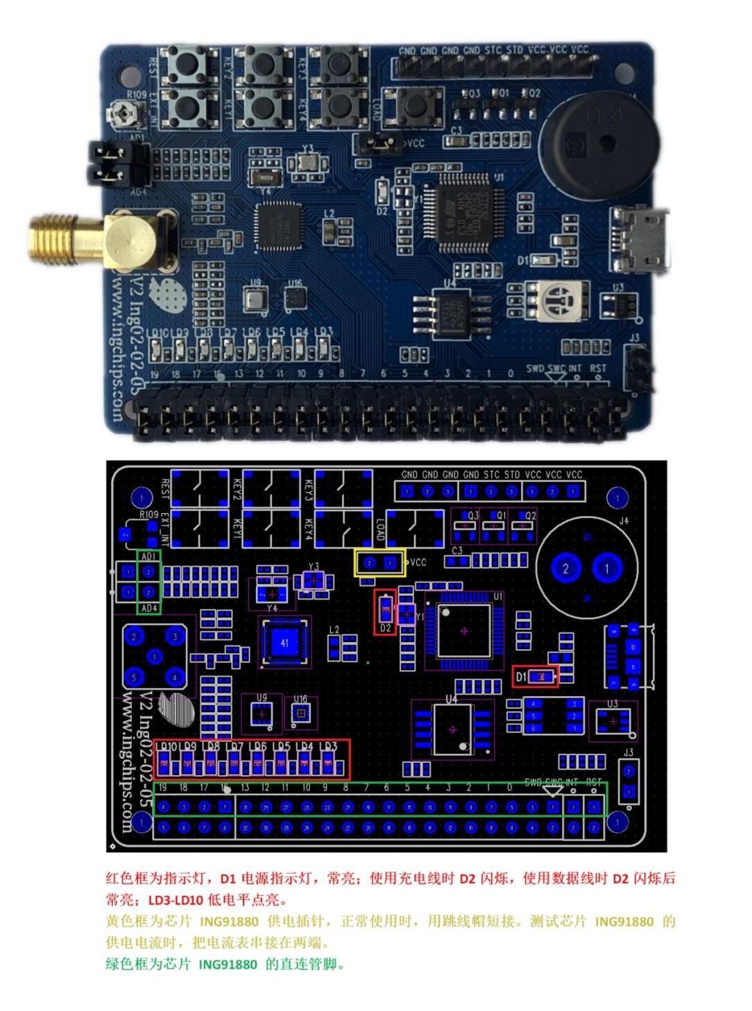
2.1、Power supply
Power supply mode: power is supplied through the micro USB interface of the development board. If it is necessary to download and debug the program, make sure to use the data cable instead of the power cable. If only the charging line is available for power supply, D2 flashes, otherwise D2 is always on;.
The development board is reserved with 2.5V external power supply interface (VCC printing on the upper right corner of EVB) and GND (GND printing on the upper right corner of the EVB). Pay attention to the current limit during power supply: when power is supplied through micro USB, the 2.5V current limit is 200mA.
2.2、GPIO
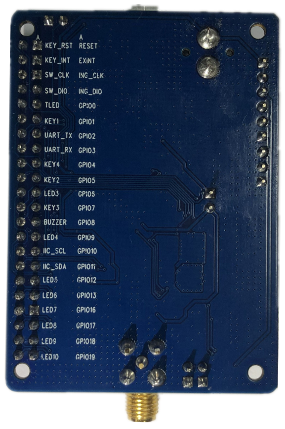
The outer row of pins on the development board are pins for off-board peripherals, the inner pins are pins from the ING91881B chip (print GPIO 0-19 corresponds to the ING91881B chip GPIO 0-19 respectively;ING_DIO and ING_CLK are SW_DIO and SW_CLK of the ING91881B chip;EXINT and RESET are EX_INT and RESET of the ING91881B chip respectively), and the outer pins near the board are temperature and humidity sensors, acceleration sensors, buttons, LEDs See the print on the back of the development board for the pin of the buzzer and other peripherals. Users either can connect specific external devices through flat cables according to needs, and configure corresponding functions through software. Or if you want to use the hardware resources on the development board, such as sensors, serial ports, buzzers and other resources, you need to use jumper caps to short circuit the corresponding positions.
For the usage of GPIO, refer to the following SDK embedded examples:(有关 GPIO 的使用方法,可参考以下示例:)
- HID Keyboard
- Peripheral ANCS
2.3、Debugging interface
The development board integrates the DAPLink (the upgraded version of CMSIS DAP) function, and supports the CDC serial port and drag and drop burning. This function is realized through a piece of STM32(The print on the development board is U1), and it communicates with the PC through the micro USB interface. The virtual serial port number is checked in the PC device manager. Before using this serial port to communicate with ING91881B, UART_TX and UART_ RX must be Short with a jumper.
SW_CLK and SW_DIO of DAPLink and The SWD interface of ING918 were connected with a jumper, and if disconnect the jumper, the EVB could be used as a DAPLink to debug other devices, or you can use other debuggers to debug the EVB. SW_CLK and SW_DIO of STM32 are led out with pins, which can be used to write STM32.
DAPLink firmware is open source.
Note: Different debuggers provide different serial port capabilities, and some debuggers may lose data when transmitting high-speed data from ING918x to PC. The ING918x can respond to serial port data immediately, so this problem does not exist when transferring from a PC to the ING918. For example, when DAPLink and J-Link OB using the same STM32 chip transmit data from ING918 to PC at 921600 baud, DAPLink does not lose data, while J-Link OB has problems.
2.4、IIC interface sensor
The development board is equipped with two sensors, BME280 and BMA280 with IIC interface, which are interconnected through the IIC1 interface of ING91881B. Before use, it is required to short IIC_SCL and IIC_SDE. BME280 is a humidity, pressure and temperature sensor, and IIC address is 0b1110110; BMA280 is a three-axis acceleration sensor with IIC address of 0b0011000.
When using the development board IIC interface sensor, pay attention to the ING91881B development board IIC_ SCL and IIC_ SDE is configured to GPIO10 and GPIO11 respectively.
For the use of the sensor, refer to the following SDK embedded examples:
- Thermometer with FOTA (Thermometer based on BME280)
- Peripheral Pedometer (Step counter based on BMA280)
2.5、LED
There are 1 tri-color LED and 8 green LEDs on the development board. The tri-color LED can be used for PWM dimming function, and the green LED can be used as the indicator (low level active). Before use, it is required to use jumper to short the corresponding pins on the EVB. The tricolor LED is controlled through the special tricolor light regulating chip TLC57931, which sends the corresponding control command through a single line, and the corresponding signal is printed TLED.
For the use of LED, refer to the following examples:
- Peripheral LED (Control tricolor LED through TLC57931)
2.6、Key
There are two kinds of keys on the development board:
1.System keys
The REST: reset button is used to reset the ING91881B.
EX_ INT: external interrupt button, press and pull it down to wake up the sleeping ING91881B.
LOAD: download key, press LOAD and burn the program, no need to press EXT_INT and RESET at the same time as required.
EXT_ INT and RESET are led out by pins. It could be selected either controlled by the KEY on board or externally through the jumper. The KEY can also control other modules.
2.Function keys
KEY1-4 can be used for other functionalities.(marked in read in Figure 1). By default, it is pulled up and pressed down to low. Before use, it is necessary to short the pins at the corresponding positions on the EVB.
For the use of keys, refer to the following examples:
- HID Keyboard
- Peripheral ANCS
2.7、Buzzer
The development board contains a buzzer with a working frequency of 4KHz. Before use, short the pins at the corresponding positions on the EVB as usual.
For the use of keys, refer to the following examples:
- Peripheral Piano
2.8、ADC
ADC interface is reserved on the development board (print AD1 AD4 on the upper left corner of the EVB). The input voltage is 1.65V when the related pins is short with the jumper (the voltage is adjustable with R109 from VCC). Users can also connect other inputs through the jumper via the inner row pins on the board.
For the use of ADC, refer to the following examples:
- Peripheral Battery
2.9、Ext_int Pin
EXTINT is an external interrupt, which is used to wake up the ING91881B in standby mode. The chip can wake up through BMA280 (short pin 1 and pin2 of J3), or through EX_INT key.
This signal has two functions:
1.During reset, assert the signal to enter the burn mode;
2.Wake the chip from the sleep mode during operation.
2.10、Chip power consumption test
The pin at the upper middle position of the development board is the external power supply pin of ING91881B. In normal use, it is shorted with a jumper. When testing the power of ING91881B, connect the ammeter in series at both ends.
3、Burn firmware
3.1、Burn with Flash Downloader
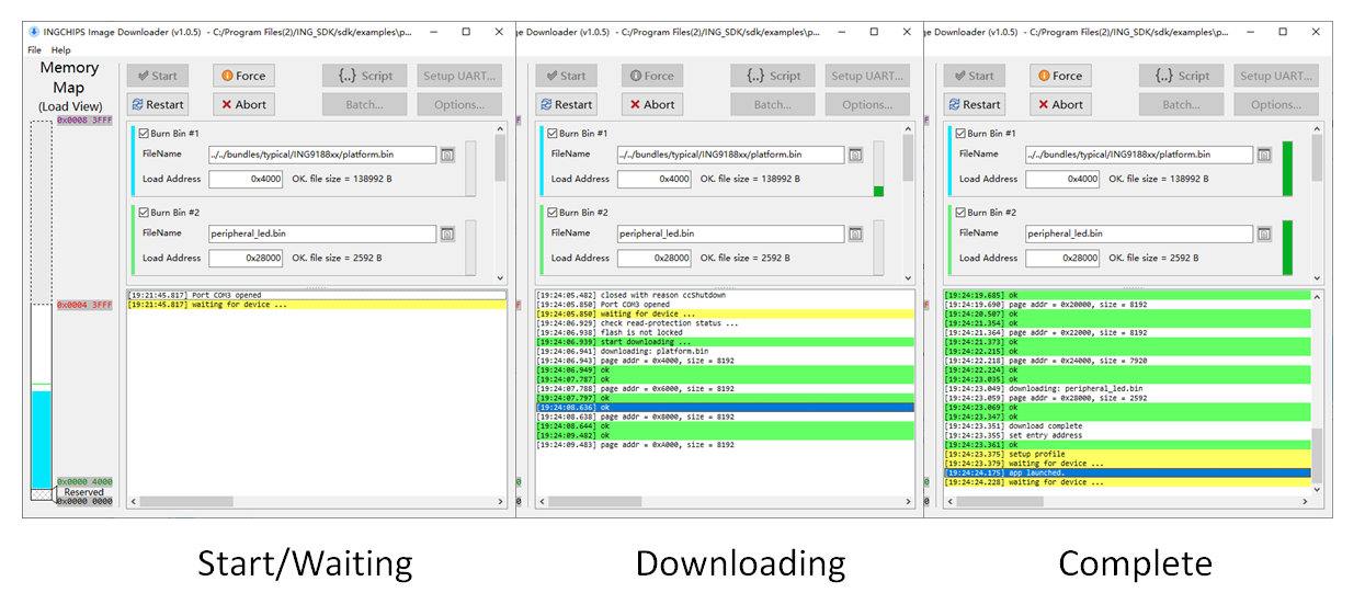
1.Find the project to download in the main interface of the ingWizard and right-click
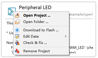
2. Select "Download to Flash..." from the pop-up shortcut menu, and the ingWizard will automatically open the Flash Downloader;
3. Click "Setup UART" in the Flash Downloader to modify the serial port number used by the development board;
4. Click "Start";
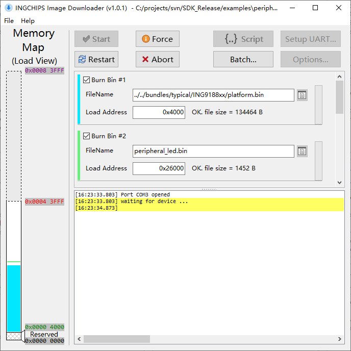
Notes:In general, a complete program contains two binary files, platform Bin (including protocol stack and real-time kernel) and App Bin. When compiling the program, only App Bin changes, platform bin does not. So platform Bin only needs to be burned once. For details, see the SDK User Guide about software architecture.
- Press the LOAD key to enter the download mode of the development board (or press RESET and EXT_INT). The interface is displayed as shown in the figure.
Notes:When released from the reset state, the Bootloader will detect the EXT_ INT, if it is high, it will enter UART download mode, otherwise it will start normally. That is to say, if you want to enter UART download mode, when the RESET button de-asserted, the EXT_NT key is asserted.
3.2、Burn with debugger
All examples can be downloaded directly through the DAPLink debugger in the IDE that supports CMSIS-DAP, for example, click "Download" directly in Keil. If the developer chooses to use the J-Link debugger, all examples can be downloaded directly from the J-Link debugger in the IDE that supports J-Link. For example, click "Download" in Keil.
Note: This method only burns the program compiled by App, not the platform Bin, so when using the development board for the first time, you should first use the Flash Downloader to completely write the platform Bin and App Bin. Some IDEs (such as CrossStudio/SEGGER) can modify settings while burning the platform Bin, but the samples in the SDK do not have this setting.
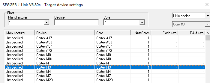
Note: If J-Link software has been installed separately, a dialog box will pop up when J-Link downloads for the first time, asking the user to select the chip type. Please select "Unspecified Cortex-M3".
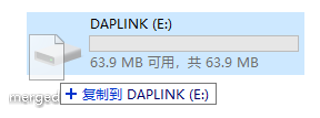
3.3、Drag and Drop Burn
The DAPLink debugger will present a USB flash disk in the computer, and copy the. bin file or. hex file (through the command line or drag and drop) to the USB flash disk to complete the burning. After the burning is completed, the USB flash disk will be remounted. Check the DETAILS in the USB flash disk TXT file, you can find that the removal count increases by 1. If the burning fails, FAIL.txt will appear, which contains detailed error information; If the burning is successful, there is no such file in the USB flash disk. Whether the burning is successful or not, the remounted USB flash disk will not "save" the burning. bin file or. hex file.
- .bin file burning
This mode only supports complete burning. The .bin file must be complete including both platform.bin and App Bin. It is recommended to automatically merge and export complete .bin files through the Flash Downloader menu item File → Merge&Export.
- .hex file burning
Intel Hex file contains address information and supports partial burning
4、Notes
- Pay attention to the current limit when supplying power to external equipment through the development board;
- Power off when adding or removing external equipment;
- Do not cover the printed board antenna with metal parts.
Quick navigation
Contact Us
Tel:010-85160285
Email:service@ingchips.com
Resume delivery:hr@ingchips.com
Office
Beijing:Room 803, Building #3, Zijin Digital Park, Haidian District
Shanghai:Room 316, Tower A, Juxin Building, Xiangke Road #58
Shenzhen:Room 1009, Shuguang Building, Science Park, Nanshan District


Technical


Developer Website

Github

Zhihu
Copyright:Ingchips Technology Co., Ltd. 苏ICP备2022018764号-2 BY : xinnet